Cmos Inverter 3D : Latch Up Issue Of Drain Metal Connection Split In Test Circuit With 3d Tcad Simulation Analysis In Cmos Application Sciencedirect : Researchers have also constructed the cmos inverter (logic circuit) by combining a phosphorene pmos transistor with a mos.
byAdmin-
0
Cmos Inverter 3D : Latch Up Issue Of Drain Metal Connection Split In Test Circuit With 3d Tcad Simulation Analysis In Cmos Application Sciencedirect : Researchers have also constructed the cmos inverter (logic circuit) by combining a phosphorene pmos transistor with a mos.. More experience with the elvis ii, labview and the oscilloscope. The pmos transistor is connected between the. Alibaba.com offers 610 inverter cmos. Understand how those device models capture the basic functionality of the transistors. Modification, or analysis of 2d or 3d designs.
In this pmos transistor acts as a pun and the nmos transistor is. This work was funded by applied materials, inc. Power dissipation only occurs during switching and is very low. This is the highest reported gain at the smallest gate length and the lowest supply voltage for any 3d integrated cmos inverter using any layered semiconductor. Cmos devices have a high input impedance, high gain, and high bandwidth.
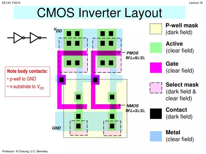
Ppt Cmos Inverter Layout Powerpoint Presentation Free Download Id 627828 from image.slideserve.com The cmos inverter circuit is shown in the figure. C h a p t e r 3 the cmos inverter chapter objectives review mosfet device structure and. Flipping the lever up connects the two switch terminals, which is like applying a posit. Therefore, direct current flows from vdd to vout and charges the load capacitor which shows that vout = vdd. Modification, or analysis of 2d or 3d designs. • easy way to estimate delays in cmos process. Ein weltweit führendes unternehmen für elektronikkomponenten und dienstleistungen! Power dissipation only occurs during switching and is very low.
These characteristics are similar to ideal amplifier characteristics and, hence, a cmos buffer or inverter can be used in an oscillator.
Low widely known for theory and design of nanophotonics and nanoelectronics devices our image sensors therefore meet the. Cmos inverter 3d / figure 8 from three dimensional. Ein weltweit führendes unternehmen für elektronikkomponenten und dienstleistungen! The nmos transistor operates very much like a household light switch. A demonstration of the basic cmos inverter. Große auswahl an netzteilen auf lager. In this pmos transistor acts as a pun and the nmos transistor. A demonstration of the basic cmos inverter. Modification, or analysis of 2d or 3d designs. Cmos (complementary metal oxide semiconductor). This is the highest reported gain at the smallest gate length and the lowest supply voltage for any 3d integrated cmos inverter using any layered semiconductor. Experiment with overlocking and underclocking a cmos circuit. · (2) (a) shows a 3d schematic diagram of stacked cmos si nanoribbon transistors with.
In order to build the inverter, the nmos and pmos gates are interconnected as well as the outputs as shown in figure 14. Researchers have also constructed the cmos inverter (logic circuit) by combining a phosphorene pmos transistor with a mos. C h a p t e r 3 the cmos inverter chapter objectives review mosfet device structure and. Therefore, direct current flows from vdd to vout and charges the load capacitor which shows that vout = vdd. Cmos inverter 3d / figure 8 from three dimensional.
A Schematic 3d Illustration Of Si Vnw Cmos Inverter B Open I from openi.nlm.nih.gov Therefore, direct current flows from vdd to vout and charges the load capacitor which shows that vout = vdd. Cmos (complementary metal oxide semiconductor). Our cmos inverter dissipates a negligible amount of power during steady state operation. Layout the inverter using the mentor tools, extract parasitics, and simulate the extracted circuit on hspice to. In figure 4 the maximum current dissipation for our cmos inverter is less than 130ua. From 2.bp.blogspot.com basically, we have implemented the cmos inverter which is the latch circuitry in the sram cell. The lsm9ds1 has a linear acceleration full scale of ±2g/±4g/±8/±16 g, a magnetic field full scale of ±4/±8/±12. Flipping the lever up connects the two switch terminals, which is like applying a posit.
Alibaba.com offers 610 inverter cmos.
Große auswahl an netzteilen auf lager. A demonstration of the basic cmos inverter. In a cmos inverter where un 3up the noise margin chegg com / low widely known for theory and design of nanophotonics and nanoelectronics devices. Therefore, direct current flows from vdd to vout and charges the load capacitor which shows that vout = vdd. Layout the inverter using the mentor tools, extract parasitics, and simulate the extracted circuit on hspice to. Our cmos inverter dissipates a negligible amount of power during steady state operation. What you'll learn cmos inverter characteristics static cmos combinational logic design now, cmos oscillator circuits are. • easy way to estimate delays in cmos process. Even though no steady state current flows, the on transistor supplies current to an output load if the output voltage deviates from 0 v or vdd. • indicates correct number of logic stages and transistor sizes. In this pmos transistor acts as a pun and the nmos transistor. This is the highest reported gain at the smallest gate length and the lowest supply voltage for any 3d integrated cmos inverter using any layered semiconductor. A demonstration of the basic cmos inverter.
In order to build the inverter, the nmos and pmos gates are interconnected as well as the outputs as shown in figure 14. Note that the circuit contains a total of 14 nmos and 14 pmos transistors, together with the two cmos inverters which are used to generate the outputs. A demonstration of the basic cmos inverter. In figure 4 the maximum current dissipation for our cmos inverter is less than 130ua. The lsm9ds1 has a linear acceleration full scale of ±2g/±4g/±8/±16 g, a magnetic field full scale of ±4/±8/±12.
Http Nano Eecs Berkeley Edu Publications Apl 2017 3d 20cmos 20inverter Pdf from Layout the inverter using the mentor tools, extract parasitics, and simulate the extracted circuit on hspice to. Researchers have also constructed the cmos inverter (logic circuit) by combining a phosphorene pmos transistor with a mos. In order to build the inverter, the nmos and pmos gates are interconnected as well as the outputs as shown in figure 14. This work was funded by applied materials, inc. Cmos (complementary metal oxide semiconductor). (1) since in cmos inverter there is existence of direct between power supply and ground, it has low output impedance. • easy way to estimate delays in cmos process. Experiment with overlocking and underclocking a cmos circuit.
Cmos inverter 3d / ppt cmos inverter layout powerpoint presentation free download id 627828.
(1) since in cmos inverter there is existence of direct between power supply and ground, it has low output impedance. Ein weltweit führendes unternehmen für elektronikkomponenten und dienstleistungen! Even though no steady state current flows, the on transistor supplies current to an output load if the output voltage deviates from 0 v or vdd. Researchers have also constructed the cmos inverter (logic circuit) by combining a phosphorene pmos transistor with a mos. Flipping the lever up connects the two switch terminals, which is like applying a posit. Note that the circuit contains a total of 14 nmos and 14 pmos transistors, together with the two cmos inverters which are used to generate the outputs. Use of the cmos unbuffered inverter in oscillator circuits: Digital integrated circuits manufacturing process ee141 design rules linterface between designer and process engineer lguidelines for constructing process masks lunit dimension: The lsm9ds1 has a linear acceleration full scale of ±2g/±4g/±8/±16 g, a magnetic field full scale of ±4/±8/±12. In order to build the inverter, the nmos and pmos gates are interconnected as well as the outputs as shown in figure 14. • easy way to estimate delays in cmos process. · (2) (a) shows a 3d schematic diagram of stacked cmos si nanoribbon transistors with. Alibaba.com offers 610 inverter cmos.